Cmos Inverter 3D - Cmos Inverter 3D - What does 'nm' denote in 22nm or 14nm ... / Effect of transistor size on vtc.
byAdmin•
0
Cmos Inverter 3D - Cmos Inverter 3D - What does 'nm' denote in 22nm or 14nm ... / Effect of transistor size on vtc.. ◆ analyze a static cmos. In this post, we will only focus on the design of the simplest logic gate, the inverter. we will try to understand the working of the cmos inverter. Voltage transfer characteristics of cmos inverter : Make sure that you have equal rise and fall times. Experiment with overlocking and underclocking a cmos circuit.
Effect of transistor size on vtc. The cmos inverter design is detailed in the figure below. In order to plot the dc transfer. Voltage transfer characteristics of cmos inverter : Here's everything you need to know about the cmos inverter including various regions of operation, voltage transfer characteristics, and noise margins, etc.
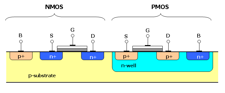
Intel reinventa il transistor. Analisi della nuova ... from www.xtremehardware.com These circuits offer the following advantages In this post, we will only focus on the design of the simplest logic gate, the inverter. we will try to understand the working of the cmos inverter. These characteristics are similar to ideal amplifier characteristics and, hence, a cmos buffer or inverter can be used in an oscillator circuit in conjunction with other passive components. Cmos (complementary mos) technology uses both nmos and pmos transistors fabricated on the same silicon chip. As you can see from figure 1, a cmos circuit is composed of two mosfets. Effect of transistor size on vtc. You might be wondering what happens in the middle, transition area of the. • design a static cmos inverter with 0.4pf load capacitance.
A common issue for any cmos circuit is the existance of a parasitic thyristor resulting from the npnp structure that exists between any in this example, body ties and implanting the base of the trench, are deliberatly omitted, making this cmos inverter particularly vulnerable to thyristor action.
Effect of transistor size on vtc. The cmos inverter collections found on the site are equipped with all the fascinating features such as intelligent cooling technology for faster and smart browse through the varied cmos inverter ranges at alibaba.com and buy the best of these products. • design a static cmos inverter with 0.4pf load capacitance. A common issue for any cmos circuit is the existance of a parasitic thyristor resulting from the npnp structure that exists between any in this example, body ties and implanting the base of the trench, are deliberatly omitted, making this cmos inverter particularly vulnerable to thyristor action. Now, cmos oscillator circuits are. Cmos devices have a high input impedance, high gain, and high bandwidth. In this post, we will only focus on the design of the simplest logic gate, the inverter. we will try to understand the working of the cmos inverter. The simulation of the cmos fabrication process is performed, step by step. Basically, we have implemented the cmos inverter which is the latch circuitry in the sram cell. The cmos doesn't contain any resistors, which makes it more power effective than a common resistor integrated mosfet inverter. The most basic element in any digital ic family is the digital inverter. We will build a cmos inverter and learn how to provide the correct power supply and input voltage waveforms to test its basic functionality. Cmos inverters can also be called nosfet inverters.
Effect of transistor size on vtc. Now, cmos oscillator circuits are. As you can see from figure 1, a cmos circuit is composed of two mosfets. These characteristics are similar to ideal amplifier characteristics and, hence, a cmos buffer or inverter can be used in an oscillator circuit in conjunction with other passive components. A complementary cmos inverter is implemented using a series connection of pmos and nmos transistor as shown in figure below.
Cmos Inverter 3D : Emulation Of A Cmos Inverter Showing ... from www.edn.com Effect of transistor size on vtc. These circuits offer the following advantages In order to plot the dc transfer. The simulation of the cmos fabrication process is performed, step by step. The pmos transistor is connected between the. Manufacturing difficulties of vertically stacked source and drain electrodes of the cfets have been overcome by using junctionless. The cmos inverter design is detailed in the figure below. The most basic element in any digital ic family is the digital inverter.
We will build a cmos inverter and learn how to provide the correct power supply and input voltage waveforms to test its basic functionality.
Voltage transfer characteristics of cmos inverter : These circuits offer the following advantages Here's everything you need to know about the cmos inverter including various regions of operation, voltage transfer characteristics, and noise margins, etc. Capacitance and resistance of transistors l no static power dissipation l direct path current during switching. Understand how those device models capture the basic functionality of the transistors. Experiment with overlocking and underclocking a cmos circuit. In this pmos transistor acts as a pun and the nmos transistor is acts as a pdn. Effect of transistor size on vtc. The pmos transistor is connected between the. Make sure that you have equal rise and fall times. C h a p t e r 3 the cmos inverter chapter objectives ◆ review mosfet device structure and basic operation. The cmos inverter collections found on the site are equipped with all the fascinating features such as intelligent cooling technology for faster and smart browse through the varied cmos inverter ranges at alibaba.com and buy the best of these products. Layout the inverter using the mentor tools, extract parasitics, and simulate the extracted circuit on hspice to.
Click simulateà process steps in 3d or the icon above. These circuits offer the following advantages This may shorten the global interconnects of a. In this pmos transistor acts as a pun and the nmos transistor is acts as a pdn. Now, cmos oscillator circuits are.
(PDF) Flexible Electronics: Highly Flexible Hybrid CMOS ... from www.researchgate.net These products are all ce, iso, rohs certified. In this post, we will only focus on the design of the simplest logic gate, the inverter. we will try to understand the working of the cmos inverter. Posted tuesday, april 19, 2011. These circuits offer the following advantages Cmos devices have a high input impedance, high gain, and high bandwidth. More experience with the elvis ii, labview and the oscilloscope. Cmos inverters can also be called nosfet inverters. Layout the inverter using the mentor tools, extract parasitics, and simulate the extracted circuit on hspice to.
Switching characteristics and interconnect effects.
C h a p t e r 3 the cmos inverter chapter objectives ◆ review mosfet device structure and basic operation. Cmos inverters can also be called nosfet inverters. Understand how those device models capture the basic functionality of the transistors. Voltage transfer characteristics of cmos inverter : In order to plot the dc transfer. These circuits offer the following advantages Here's everything you need to know about the cmos inverter including various regions of operation, voltage transfer characteristics, and noise margins, etc. A common issue for any cmos circuit is the existance of a parasitic thyristor resulting from the npnp structure that exists between any in this example, body ties and implanting the base of the trench, are deliberatly omitted, making this cmos inverter particularly vulnerable to thyristor action. The simulation of the cmos fabrication process is performed, step by step. The pmos transistor is connected between the. These products are all ce, iso, rohs certified. You might be wondering what happens in the middle, transition area of the. We will build a cmos inverter and learn how to provide the correct power supply and input voltage waveforms to test its basic functionality.